SURFACE GRID COUPLER SUITABLE FOR PHOTONIC DEVICES, ASSOCIATED METHOD AND ASSEMBLY WITH SURFACE GRID COUPLER
Description
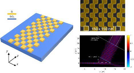
The silicon on insulator (SOI) platform is one of the most popular platforms for the implementation of compact integrated photonic devices due to its compatibility with CMOS manufacturing processes and its high index contrast. An important consequence of the small size of the waveguides built on this platform is the difficulty of light coupling between the optical fiber and the chip. To solve this problem, two types of couplers are usually used: edge couplers and surface grid couplers. The latter provide more tolerance for alignment errors of the optical fiber and provide more flexibility, since the coupling occurs vertically and the coupler can be located at any point on the surface of the chip. However, in typical grid couplers there is a rigid trade-off between obtainable bandwidth and efficiency, such that both performances cannot be maximized. One possible solution is a type of surface grating coupler called a “zero-order coupler.” In this case, the device consists of a periodic structure in the subwavelength grating (SWG) regime that acts as an equivalent metamaterial guide. With the convenient geometry design of this SWG guide, light is evanescently coupled between the guide and a silicon prism placed on top of it. Although zero-order couplers allow obtaining a coupling efficiency of 90% or more and a bandwidth around 100 nm, this is limited by the chromatic dispersion of the SWG guide. The present invention solves this obstacle by replacing the common SWG guide with a “bricked” SWG guide. In this way, the dispersion with the wavelength of the guide is drastically reduced, which allows the range of operating wavelengths to be significantly widened without sacrificing the coupling efficiency of the device.
Advantages
The main novelty of the invention is the bandwidth offered, which triples that of previous fiber-chip couplers based on zero-order radiation and is more than seven times greater than that of conventional surface grating couplers on the SOI platform. At the same time, this notable increase in bandwidth is accompanied by a radiation efficiency close to 90%, making the device the fiber-chip per surface coupler with the highest bandwidth-efficiency product to date. Furthermore, the device can be manufactured using standard lithography and in a single etching step, without requiring the introduction of reflectors, multiple guiding layers or complex geometries.
Uses and Applications
The present invention falls within the field of integrated optics. The proposed device and method can be used in all those applications in which it is necessary to inject light into a photonic chip vertically (not through the edge of the chip), in a wide range of wavelengths or with high efficiency. Examples of these applications are optical communications using wavelength division multiplexing techniques or quantum communications.
Keywords
Sectors
Areas
Patent Number
ES3021132A1 Expediente
Applicants
UNIVERSIDAD DE MÁLAGA
Inventors
ALEJANDRO SÁNCHEZ POSTIGO, ALEJANDRO ORTEGA MOÑUX, JUAN GONZALO WANGUEMERT PEREZ, IÑIGO MOLINA FERNANDEZ, ROBERT HALIR , JOSÉ MANUEL LUQUE GONZÁLEZ, ABDELFETTAH HADIJ EL HOUATI
Filing Date
23/11/2023
Protection Level: National (Spain)
Processing Status: Spanish protection application


