HIGHLY DIRECTIONAL OPTICAL PLANAR DIFRACTIVE DEVICE
Description
Silicon photonics allows the development of integrated optical structures that, being based on silicon and derived materials, offer high levels of miniaturization and can be manufactured following standard processes of the microelectronics industry. In general, photonic chips require the use of devices that facilitate light coupling between the integrated structures and the external environment. In multiple applications, such as quantum communications or remote sensing, it is necessary that the couplers used be ultra-efficient, to avoid degradation of the transmitted and received optical signals. Surface grating couplers are commonly used to couple light to optical fibers or photodetectors, while phase-coupled optical antennas are more common for cases where the goal is to direct the emitted light toward remote objects. With common guidance platforms, silicon on insulator (SOI) and silicon nitride on insulator, typical efficiencies hardly exceed 60%, since a significant portion of the light that should be diffracted away from the chip is radiated onto the chip. the substrate. To solve this problem, advanced techniques have been implemented, among which are the introduction of metal mirrors in the substrate, to recover that fraction of light that is lost, or the modification of the geometry of the radiating elements, to maximize the percentage of light diffracting into the air. However, these methods involve complex and expensive manufacturing techniques.
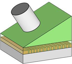
The present invention shows a new family of coupling devices that can be manufactured using typical lithographic technologies and with which theoretical efficiencies of 100% are achieved. To do this, the surface grating couplers or optical antennas in SOI are coated with silicon nitride or a material with a relatively high refractive index, in such a way that, with the appropriate design, the coupling condition is met only between the layer guide layer and the cover, and not between the guide layer and the substrate. To allow light to be transmitted into the air, a prism made of a material with a refractive index equal to or similar to that of the cover is placed on the cover. Additionally, reflections between the prism and the air are minimized with an anti-reflective film. Once the amount of light radiated into the air has been maximized, the geometry of the structures is appropriately designed to maximize the performance of the device. For example, for chip-fiber coupling, the properties of the radiating elements are gradually varied through an apodizing process based on periodic structures in the subwavelength grating (SWG) regime, so that the profile of the radiated field and the mode profile of the optical fiber match, which avoids additional power losses. In the case of optical antennas, they must be carefully arranged in an array to adjust the phase coupling between them and thus provide beam steering capability. The materials used in these proposed embodiments are mere examples and could be replaced by others to achieve high coupling efficiencies in other guidance platforms, provided that the design method described in the present invention is used.
Advantages
The key aspect of this invention is the high coupling efficiency obtained, which is close to 100% without requiring reflectors, multiple guiding layers, three-dimensional geometries or lithography manufacturing processes with more than one etching step. On the other hand, for applications in which wavelength sweeps are used to steer radiated beams, phase-coupled optical antennas have an amplified scanning speed by a factor of up to ~2 compared to other optical antennas in SOI technology.
Uses and Applications
This invention belongs to the field of integrated optics. The proposed devices and methods can be used in applications that require light coupling between a photonic chip and an external element or medium. Examples of use include ultra-efficient fiber-to-chip or fiber-to-surface photodetector couplers for applications based on quantum technologies, chip interconnection systems in data centers, or phase-coupled optical antennas for satellite communications, autonomous vehicles, and LiDAR. .
Keywords
Sectors
Areas
Patent Number
WO2025109533 Expediente
Applicants
UNIVERSIDAD DE MÁLAGA, NATIONAL RESEARCH COUNCIL CANADA
Inventors
ALEJANDRO SÁNCHEZ POSTIGO, PABLO GINEL MORENO, JENS HOLGER SCHMID , ABDELFETTAH HADIJ EL HOUATI, PAVEL CHEBEN , IÑIGO MOLINA FERNANDEZ, JUAN GONZALO WANGUEMERT PEREZ, ALEJANDRO ORTEGA MOÑUX, ROBERT HALIR
Filing Date
23/11/2023
Protection Level: Worldwide (PCT countries)
Processing Status: Wordwide (PCT countries) protection application


